
CNI Tool
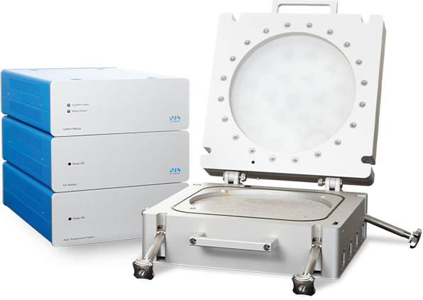
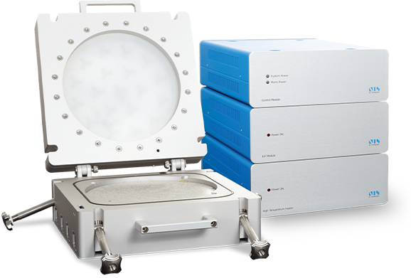
Compact Nanoimprint Tool (CNI)
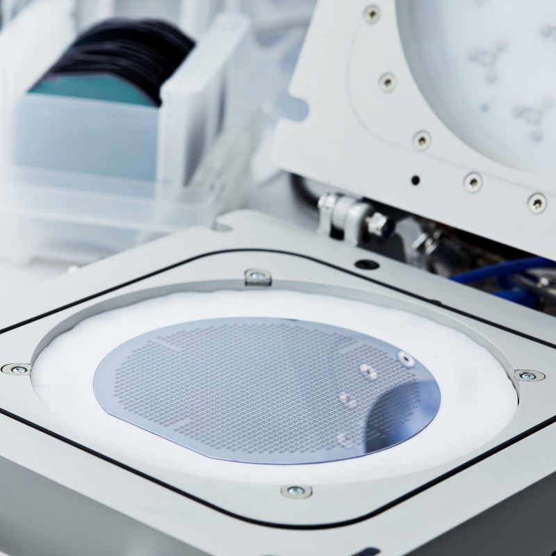
Our CNI is the perfect desktop tool for easy replication and nanoimprint of micro and nanoscale structures. Designed with flexibility in mind, our system is available in 20 different configurations (chamber sizes, UV exposure, and temperature ranges) to meet your specific requirements—making it easy to find the ideal solution for your research.
CNI 120
Flexible for R&D and lower cost
Designed for substrates up to 100 mm. Its compact format provides maximum process flexibility, making it ideal for technology development, process optimization, and low-to-medium volume output.
The CNI 120 enables customers to accelerate innovation while minimizing development costs and material consumption.
CNI 210
Larger format nanoimprint for advanced optics
Enables nanoimprint patterning on substrates up to 200 mm, supporting the production of larger optical components and higher device counts per substrate.
Designed for customers moving beyond early-stage development, the platform combines the precision and fidelity required for advanced optical structures with the substrate size needed for manufacturing-oriented workflows.
Advantages
- Easy to install
Plug and play in less than 20 minutes - Easy to use
Everyone can use it. But we also offer individual support if you need it - Versatile and flexible
The CNI tool is unique in its offering and supports many different technologies and processes
- Compact size, big utility
A desktop size tool that can work with any size of stamp and substrates up to 210 mm (8” round) - High quality imprints
Capable of replicating and nanoimprinting structures from smaller than 40 nm to structures larger than 100 µm
Options
| You have a choice | Options |
|---|---|
| Chamber sizes | 120 mm or 210 mm round |
| UV source and wavelength | None. Or choice of 365 nm, and/or 405 nm |
| Heating | None, Or 200°C or 250°C maximum temperature |
| Touch computer | Included with both versions |
| Consumables | Available to purchase separately |
Use Cases & Features
| Use Cases | Features |
|---|---|
| Nanostructure imprinting | Manual load and unload of stamp and substrate |
| Microstructure imprinting | Automatic process control |
| High-resolution grating replication on silicon | Easy to operate software interface |
| Imprinting on fragile substrates | System logs all recipes and processes |
| Working stamp fabrication | Imprint pressure from 0.3 to 11 bar |
| Hot embossing of high-aspect-ratio features | Imprint in vacuum (1 mbar) |
| Hot embossing of polymer sheets | |
| Thermal polymer bonding |
Lots more, just ask.
User Stories
“We have a very special sample set up which differs from standard applications. To process these samples, we were looking for a tool that allowed us to perform nanoimprinting at elevated temperatures and high forces under vacuum conditions.”
“We were really happy when we found the CNI tool. It combined all our requirements with an open construction and a flexible nature, enabling us to manipulate our sample setup inside the tool easily.”
– Enno Schatz, University of Würzburg (now CTO at NanoStruct)
Contact Us
Whether you’re ready to manufacture a design or need help developing one, NILT can help you find a path from concept to production.